Last semester, I took an honors colloquium for CS 335: Inside the Box: How Computers Work. The main section of the class was all about the different levels of technology that goes into a computer, from how transistors work to logic gates to processor components and more. For the colloquium project, I teamed up with Sagnik Pal to build an 8 bit computer out of some (not so) basic chips.
Separating the modules
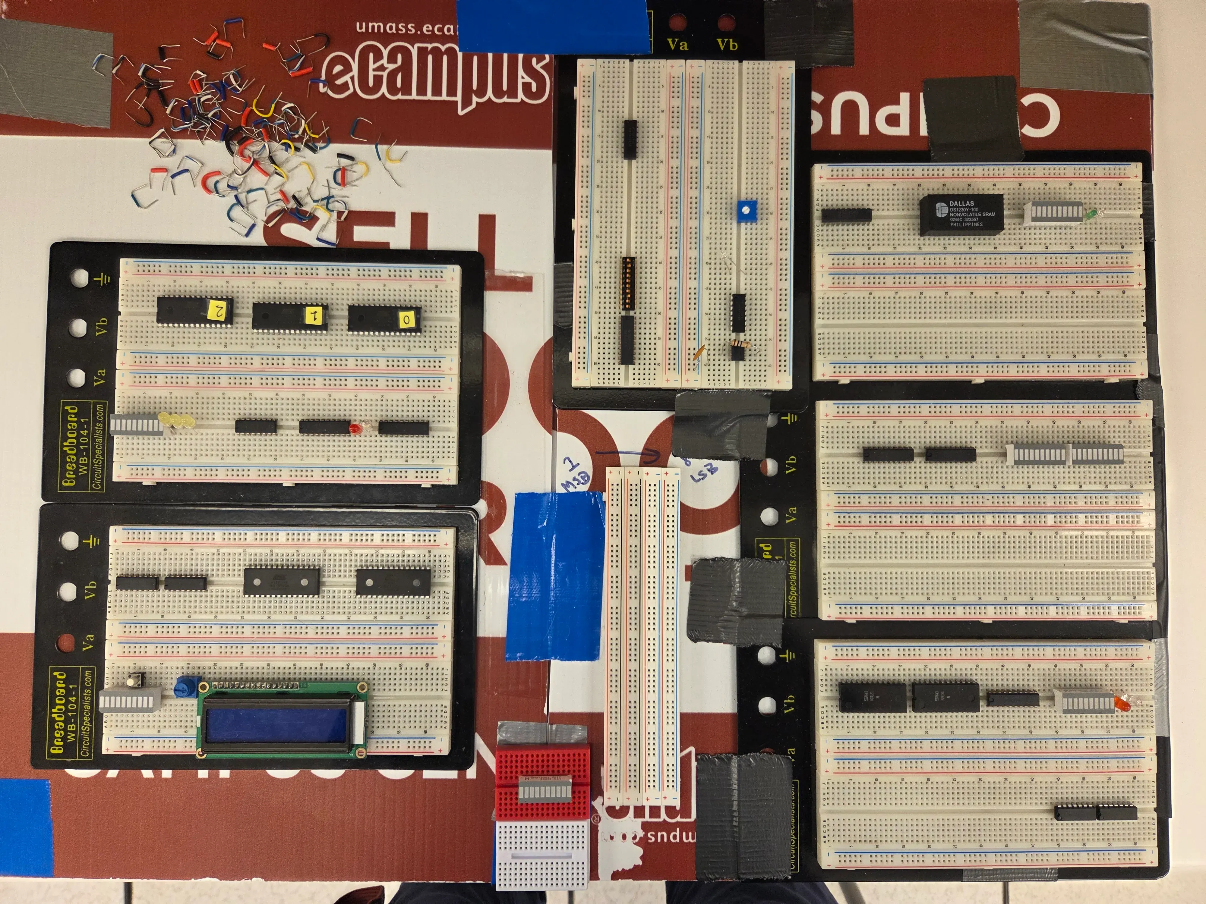
For this tutorial, you will need one (1) 8 bit computer. (Unfortunately, I only remembered to take photos as I was disassembling it). If you want to build an 8 bit computer, you can follow these steps in reverse order.
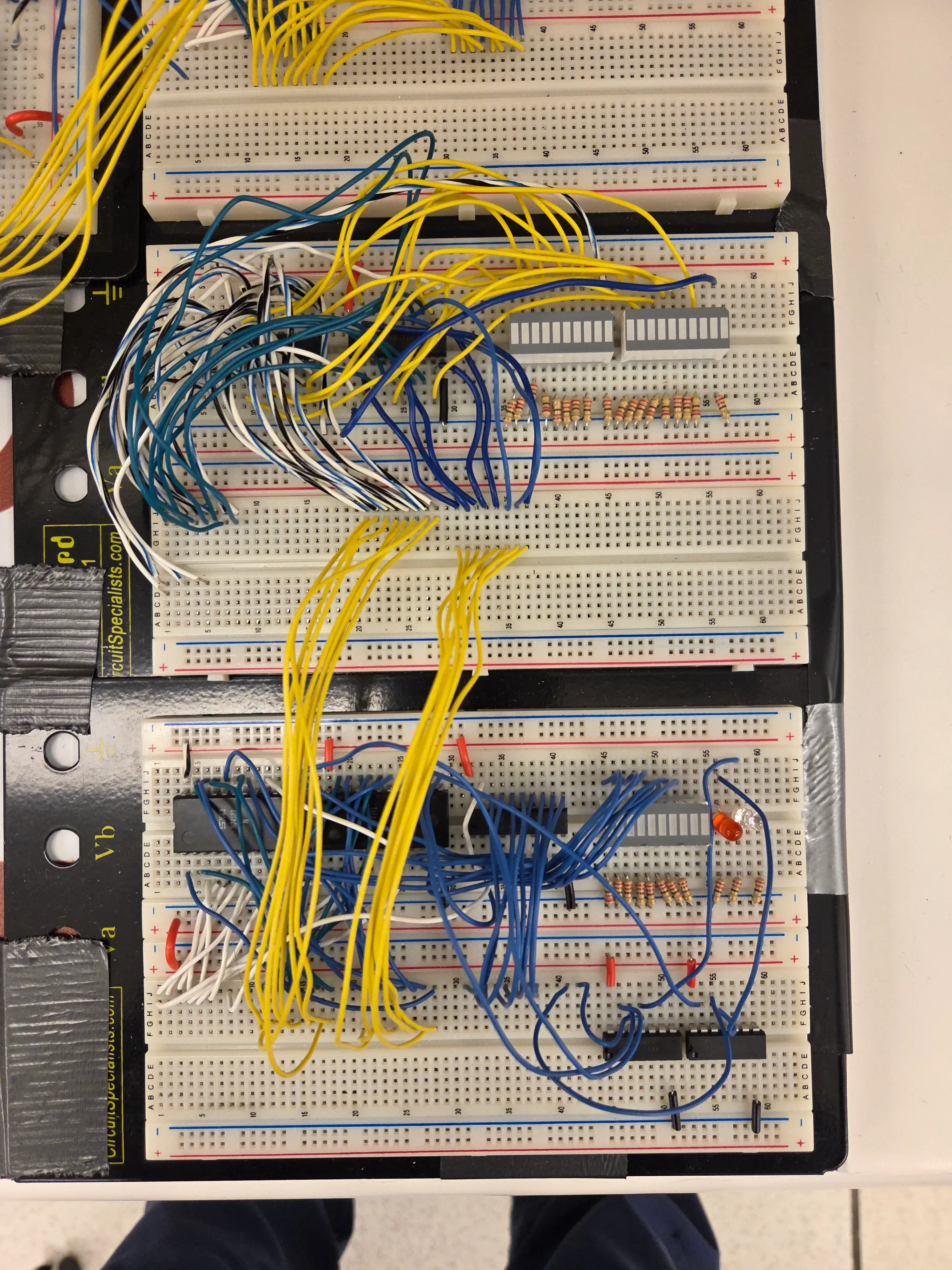
Our whole computer consists of 8-9 main modules:
- clock
- RAM
- registers
- ALU
- LCD display
- program ROM + program counter
- instruction decoder
- the bus
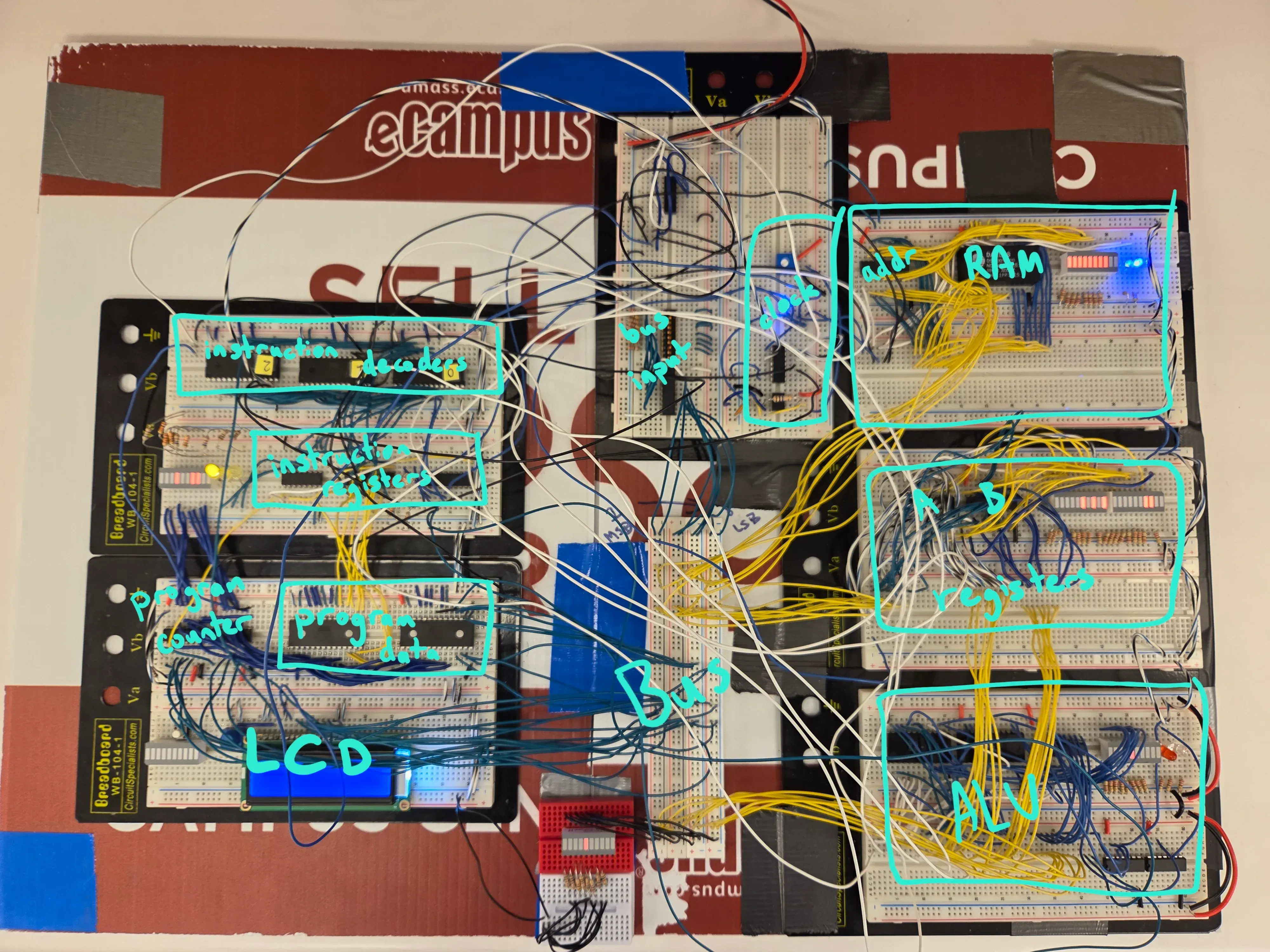
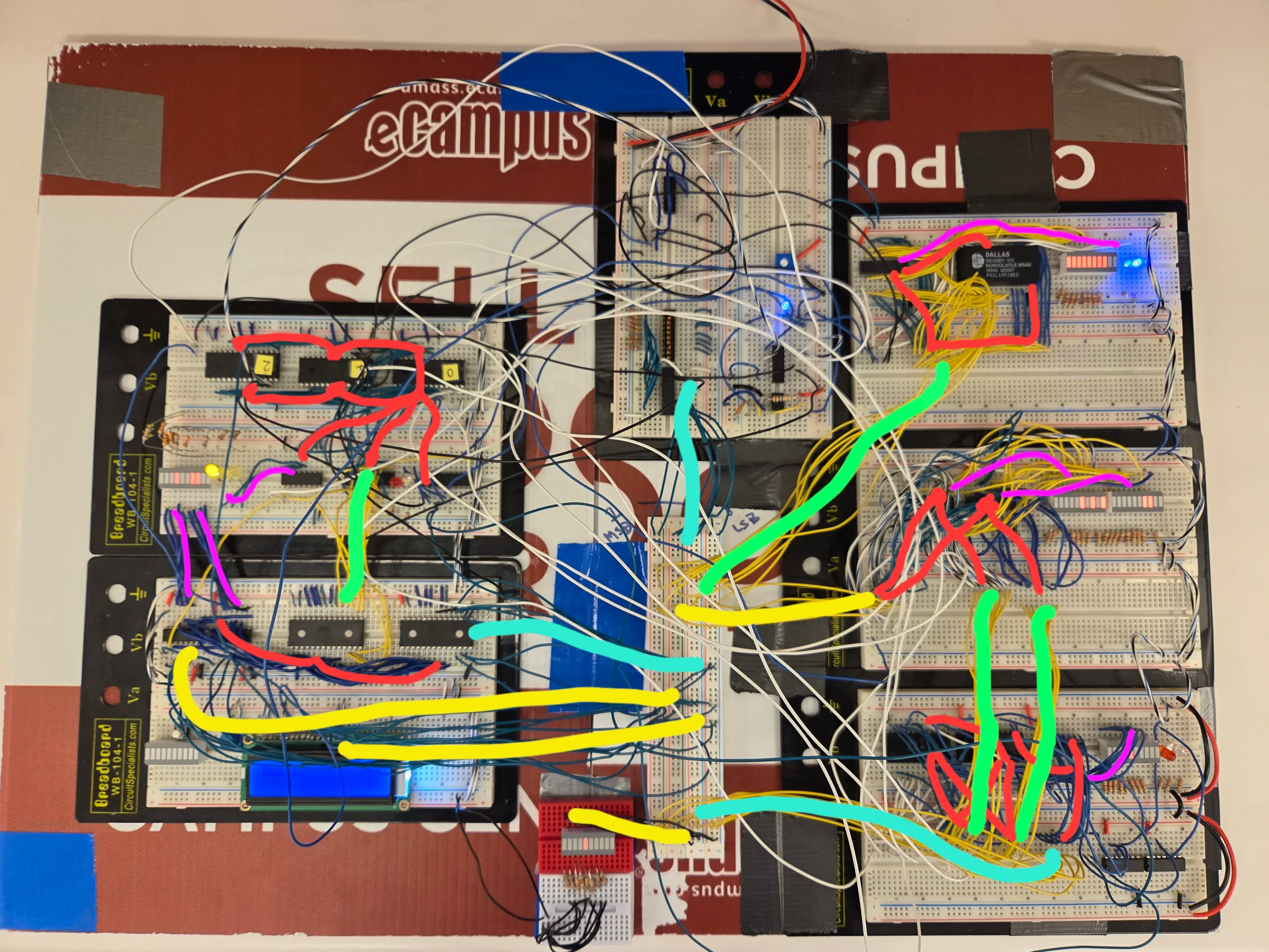
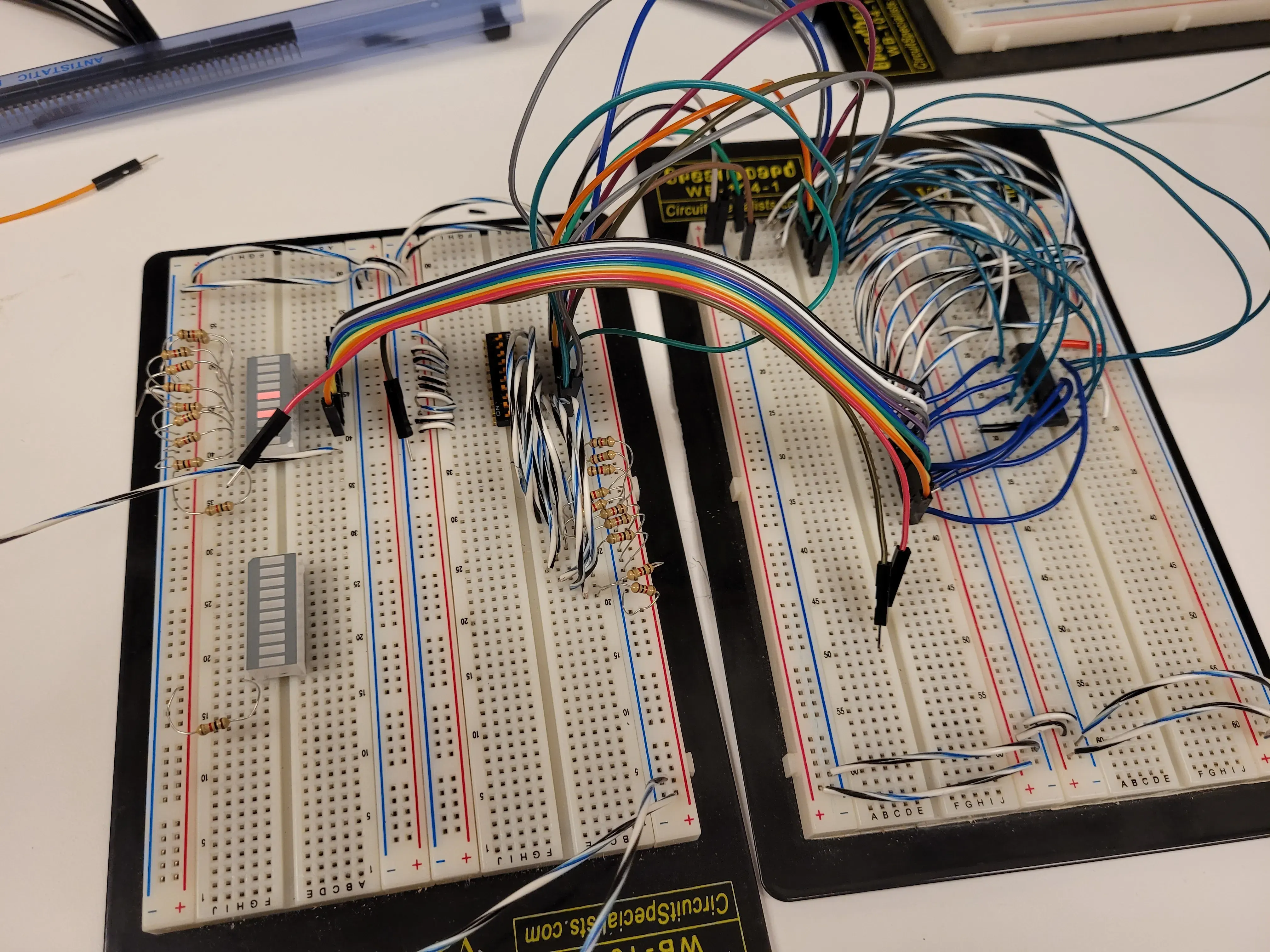
Spanning between these modules are control signal wires, data wires, and power wires. Everything else is (mostly) self contained in each of the modules.
yellow: bus output (module input)
cyan: bus input (module output)
green: i/o (between modules or on bus)
red: intra-module data lines
magenta: status/display wires
control signal wires are omitted for clarity
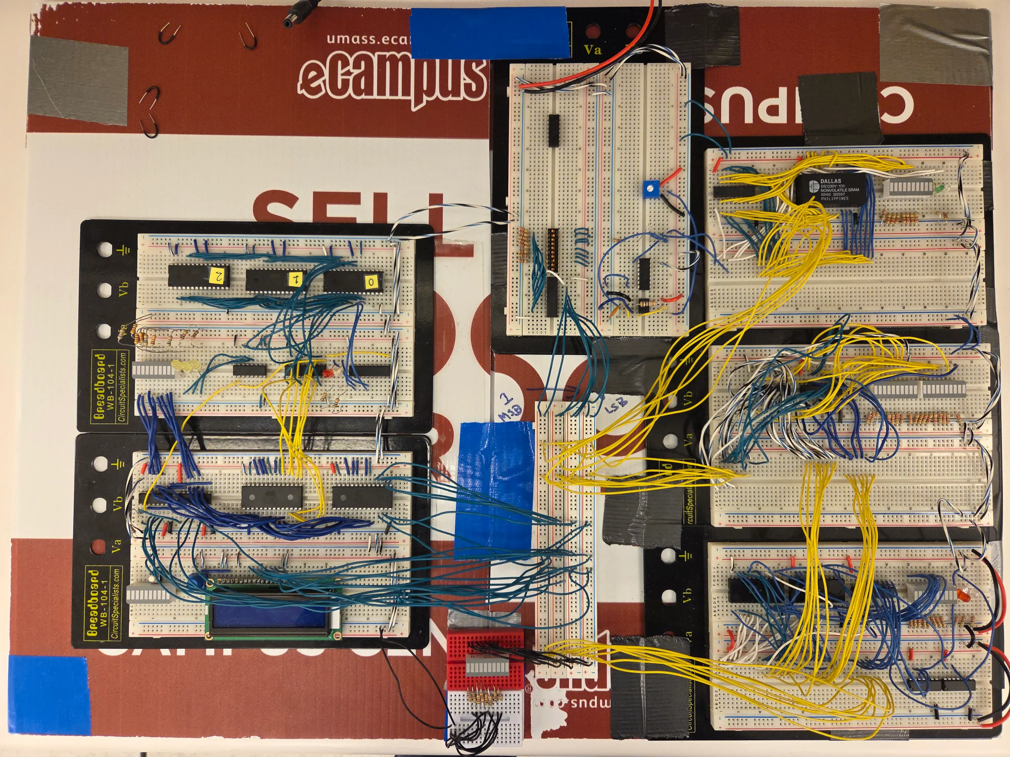
Removing control signal wires and the bus
The first step in disassembling the 8 bit computer is to remove all the control signal wires. These connect every module to the instruction decoder/control unit and the clock, so you want to get rid of them first so they don’t get in the way of the rest of the disassembly.
Now it’s a lot easier to see each of the modules and their connections.
At this point, if you ever want to debug your computer, you can wire the signals to positive/negative power manually and single step the clock. This helps a lot when trying to debug whether each instruction has the right control signals.
We can also remove the wires connecting everything to the bus. In this basic computer, there is a single bus that all data is passed through, including ALU outputs, RAM addresses, program constants/immediates, and more.
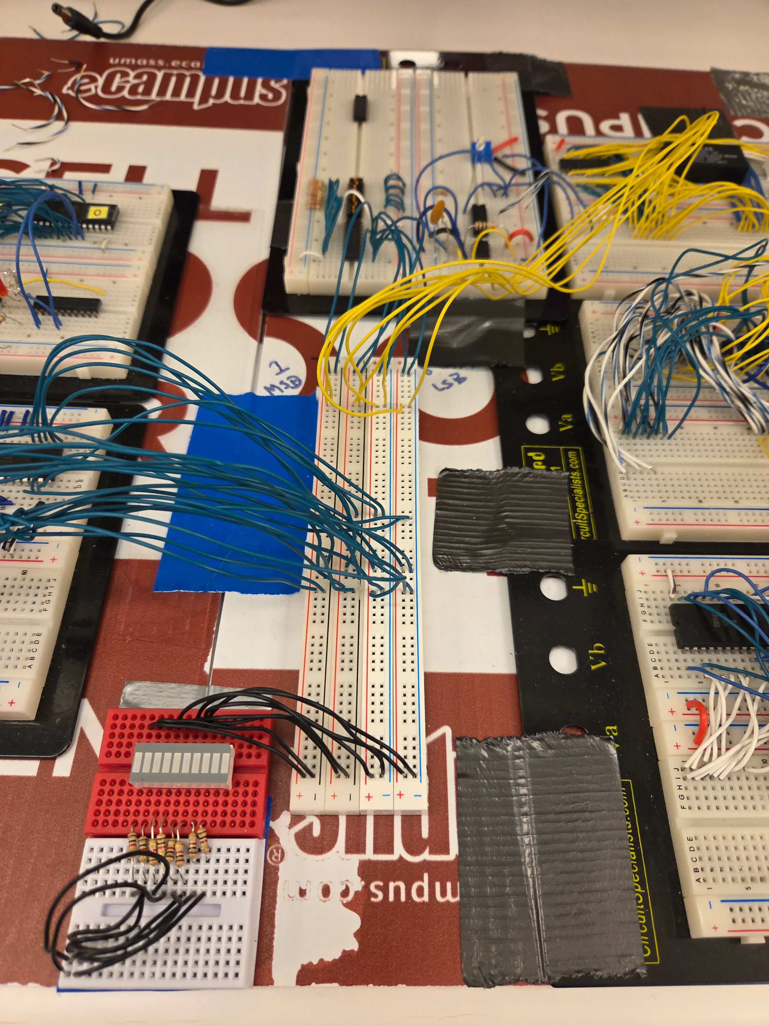
Now, we are left with the individual module groups.
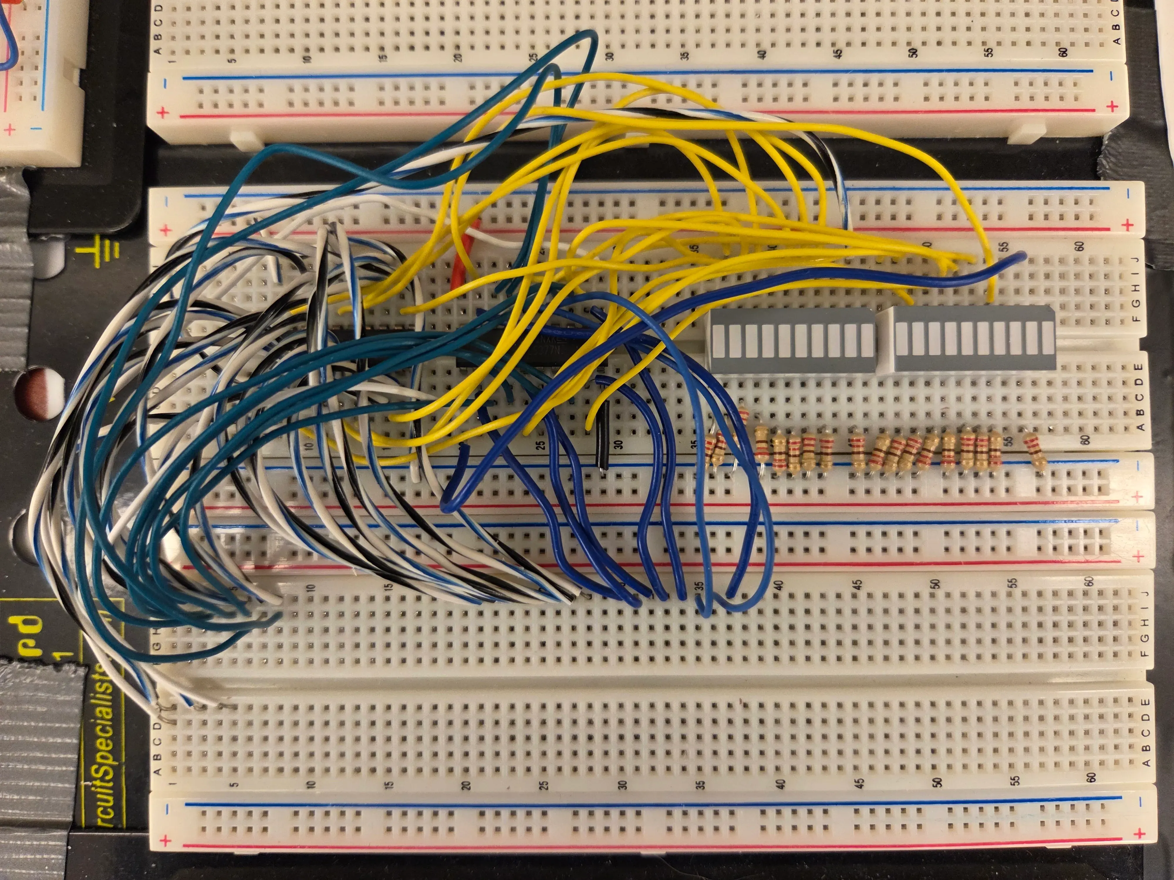
The registers and ALU
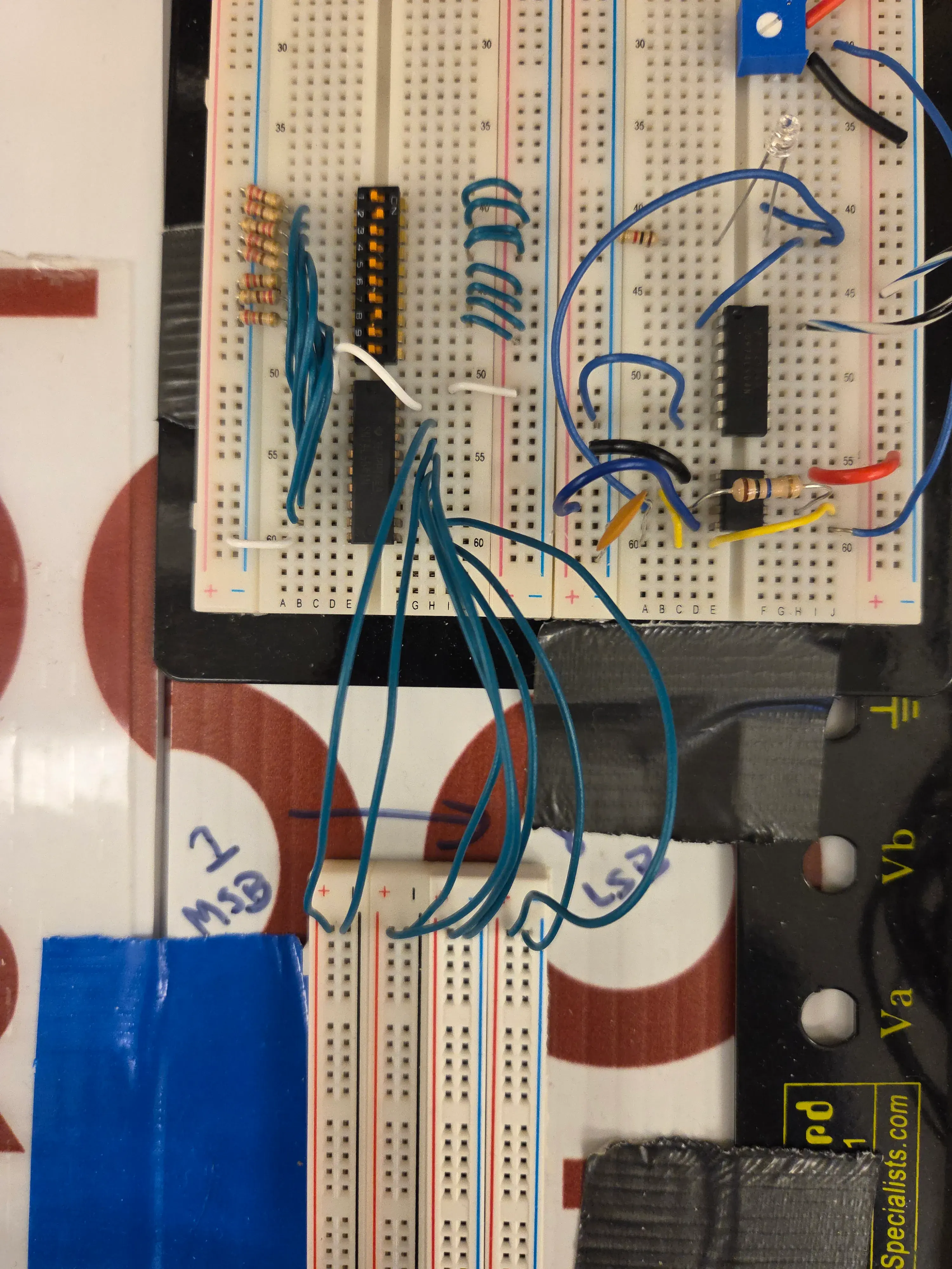
In this computer, we had 2 registers and 1 ALU.
 The two yellow wire groups in the image above connect the outputs of the two register chips to the inputs of the ALU.
Removing the connecting wires between the two boards shows the inputs/outputs for each board more clearly.
The two yellow wire groups in the image above connect the outputs of the two register chips to the inputs of the ALU.
Removing the connecting wires between the two boards shows the inputs/outputs for each board more clearly.
Our register module contains 2 74377 chips, and have the following i/o:
- control signals: clock, write register A, write register B
- input: 8 bit data in
- output: 8 bit register A, 8 bit register B
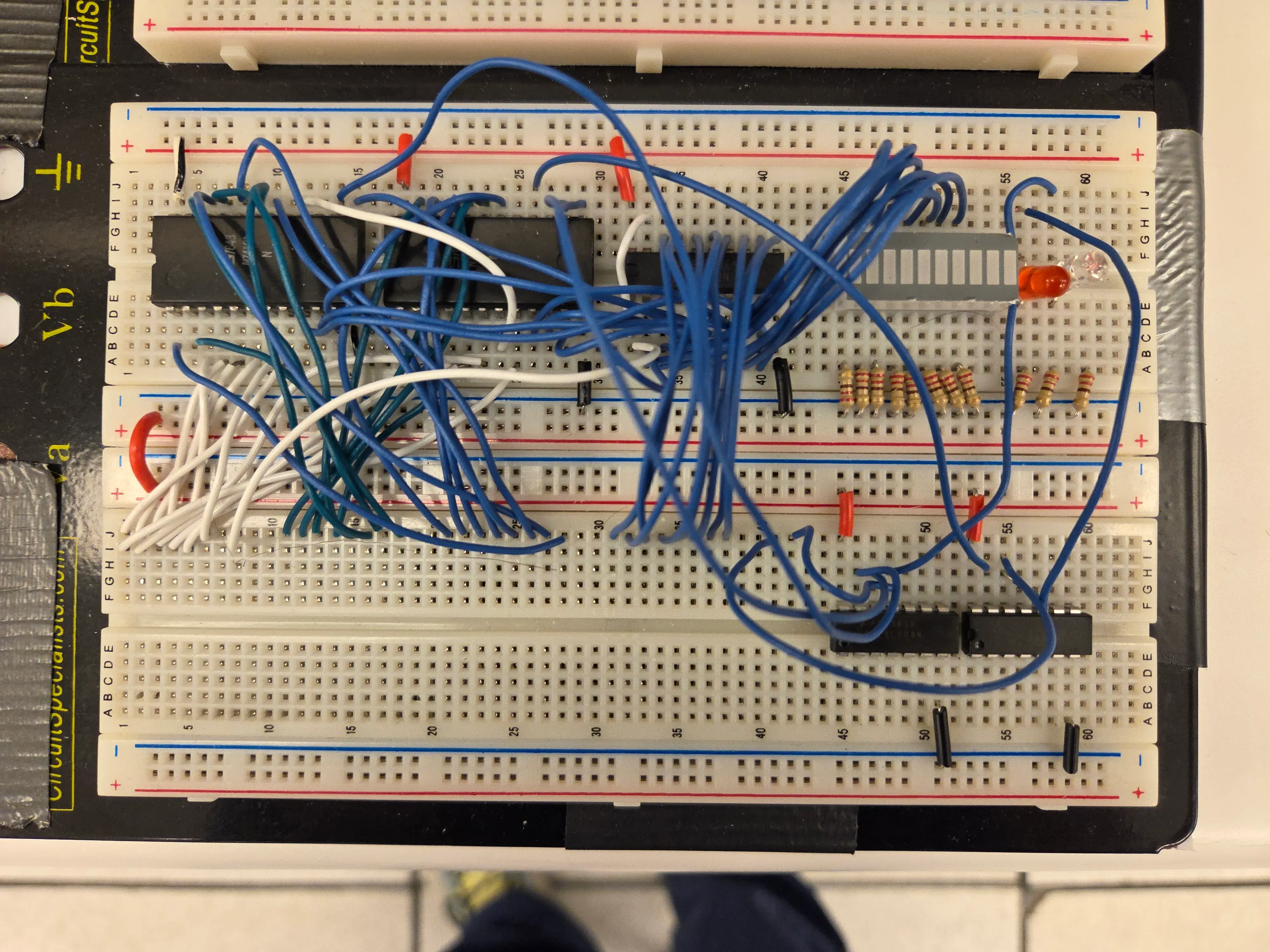
For the ALU we chained 2 4 bit sn54s181 ALUs together. Unfortunately, they did not have much of the functionality we wanted, so we had to add a 74541 buffer to enable/disable output and some logic gates to get comparisons and carry flags. Additionally, the comparison/subtract functionality required a different carry in, so we needed to add a control signal for that. Notably, there is no clock input, since the ALU does not need to store any data.
The i/o is as follows:
- control signals: 5 bit ALU function, 1 bit carry in, output enable/disable
- input: 8 bit register A, 8 bit register B
- output: 8 bit result, carry/ge flag, zero flag
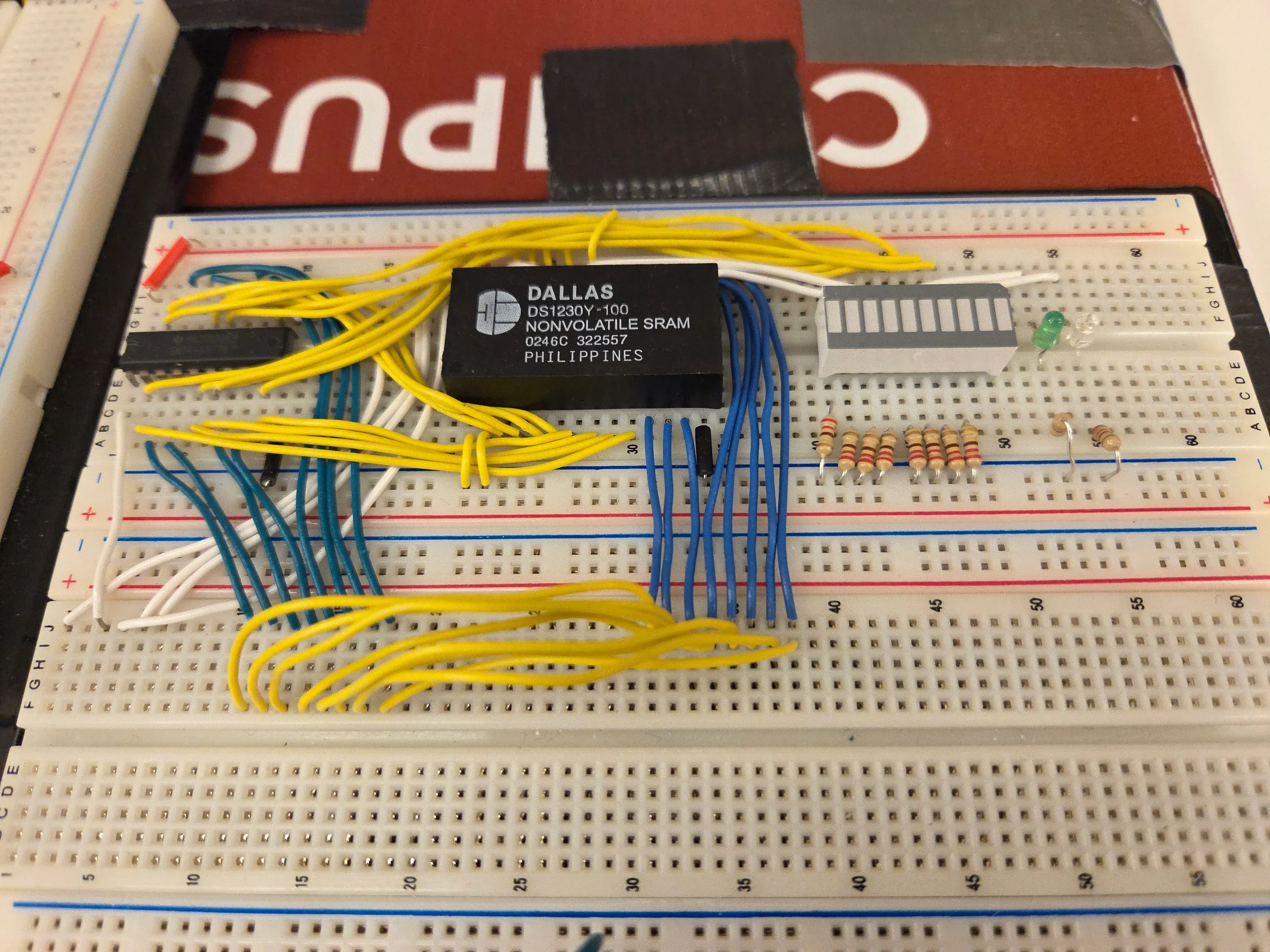
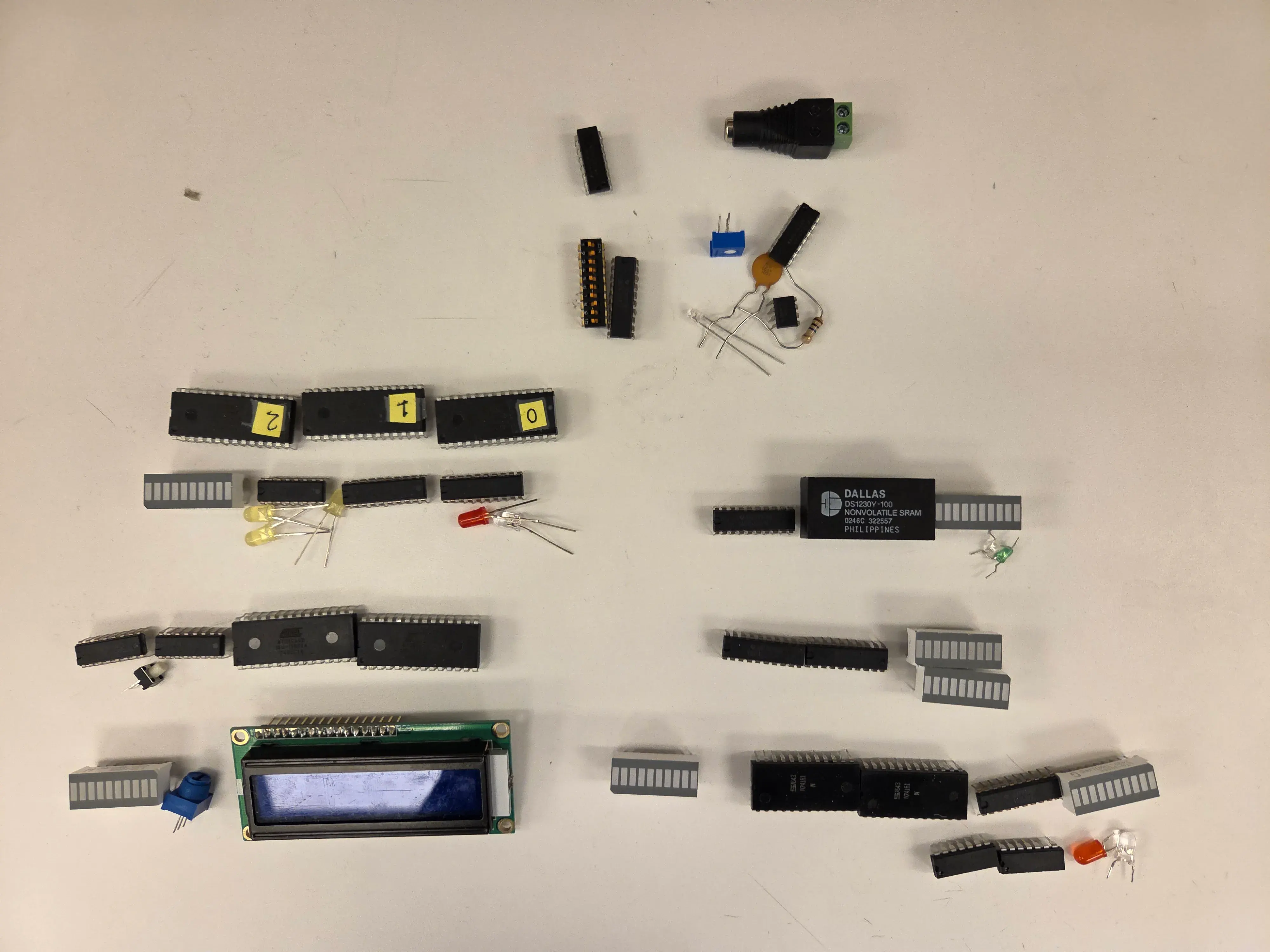
The RAM
Chip Weems had some NVRAM lying around, so we just used one of them. They had a 13 bit address space, so we just wired 5 of the bits to ground and used the other 8 for our addresses. To hold the address, we just used another 74377 register chip. The data in/out was the same on the RAM chip, but it didn’t matter that much since we made our control signals such that we can’t read and write at the same time.
The i/o is as follows:
- control signals: clock, write RAM address, write RAM, read RAM, enable RAM
- input/output: 8 bit data line
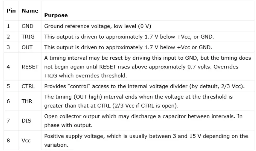
The clock
The clock was simultaneously the simplest yet hardest module to get correct. Many tutorials online for 555 timers used different confusing schematics, and the datasheet’s pinout descriptions were not helpful. Additionally, we had to tinker around with the potentiometer, resistor, and capacitor values until we got a steady blinking on the LED. There is both a clock and an inverted clock, but we only ended up using the clock.
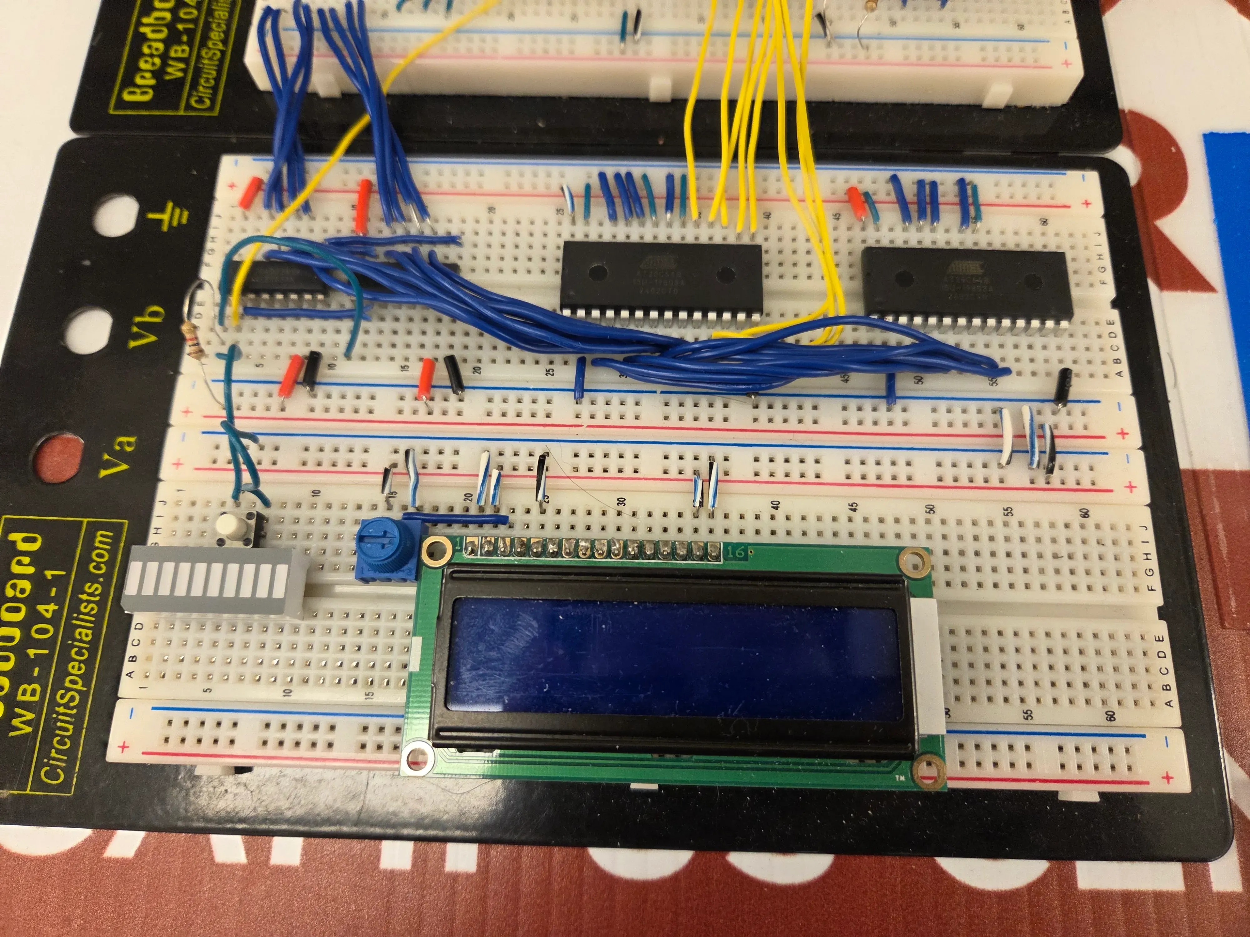
ROM + PC
To hold program data, we used 2 EEPROMs: 1 for instructions, and 1 for immediate fields/data. They had 13 bit address spaces, but we only used 8 bits, restricting our program sizes to 256 bytes. For the program counter (PC), we used 2 74173 chips, allowing for easy incrementing. As you can see, the program counter output is tied to the EEPROM address. Since the EEPROMs had an enable pin, we could wire the data ROM output to the bus and the instruction ROM output to the instruction decoder.
The i/o is as follows:
- control signals: clock, PC increment, PC write (jmp), PC reset button, data out enable
- input: 8 bit jmp address
- output: 8 bit instruction (to instruction decoder), 8 bit immediate/data
Instruction decoder
The instruction decoder, like the program data, used more EEPROMs. Here, we used them to map each instruction (8 bit) to control signals (~20 bits). We also used a 3 bit subclock so each instruction could have multiple parts (fetch, add, store, etc), as well as two flags (carry/ge and zero) for conditionals. These totaled to 13 bits of address space, which the EEPROMs fit perfectly. The subclock used a 74173 chip, just like the program counter, and was tied to reset when the PC increment signal was on. The flags used a 74377 chip (even though we only used 2/8 bits) and was tied to the ALU.
The i/o is as follows:
- control signals: clock, subclock reset, instruction write, flag write
- input: 8 bit instruction, 2 bit flags
- output: all control signals for other modules
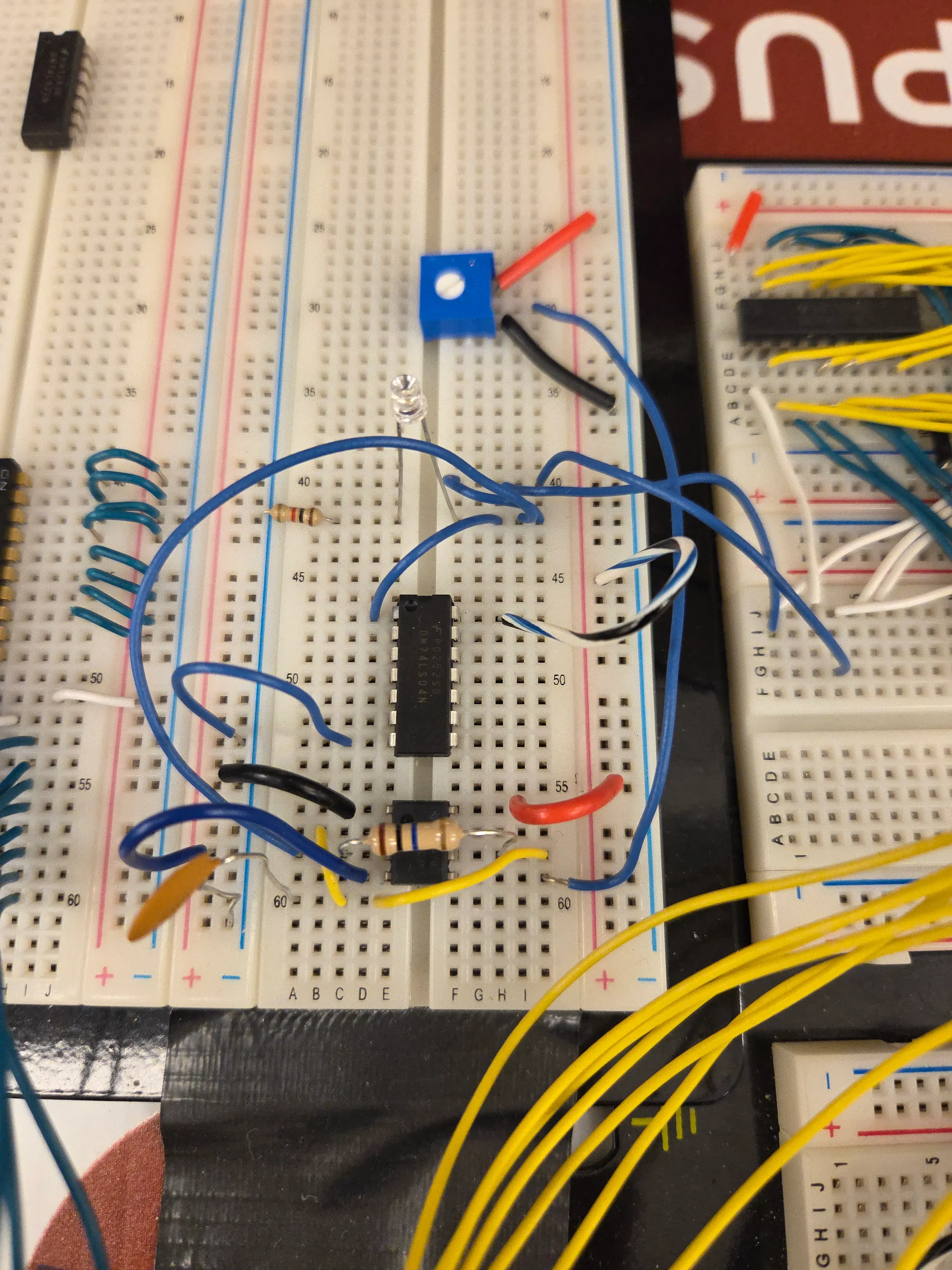
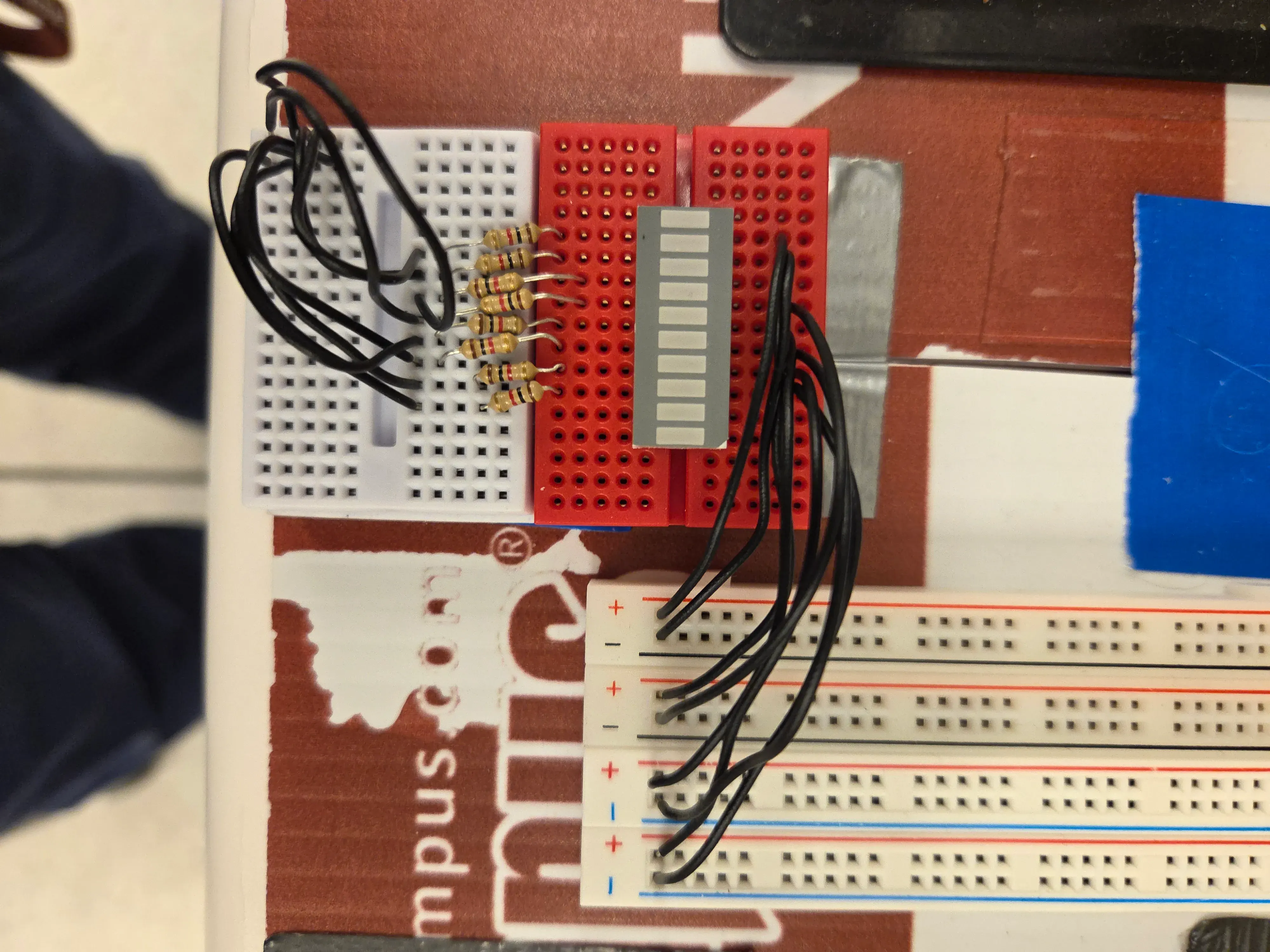
LCD display
We also found this 16x2 LCD display (A-1748/1602d1, I couldn’t find any links) in Chip Weems’ miscellaneous project parts boxes, and since it used an 8 bit data input, we figured that we could fit it into our computer. The i/o is as follows:
- control signals: write LCD data, write LCD control data
- input: 8 bit data
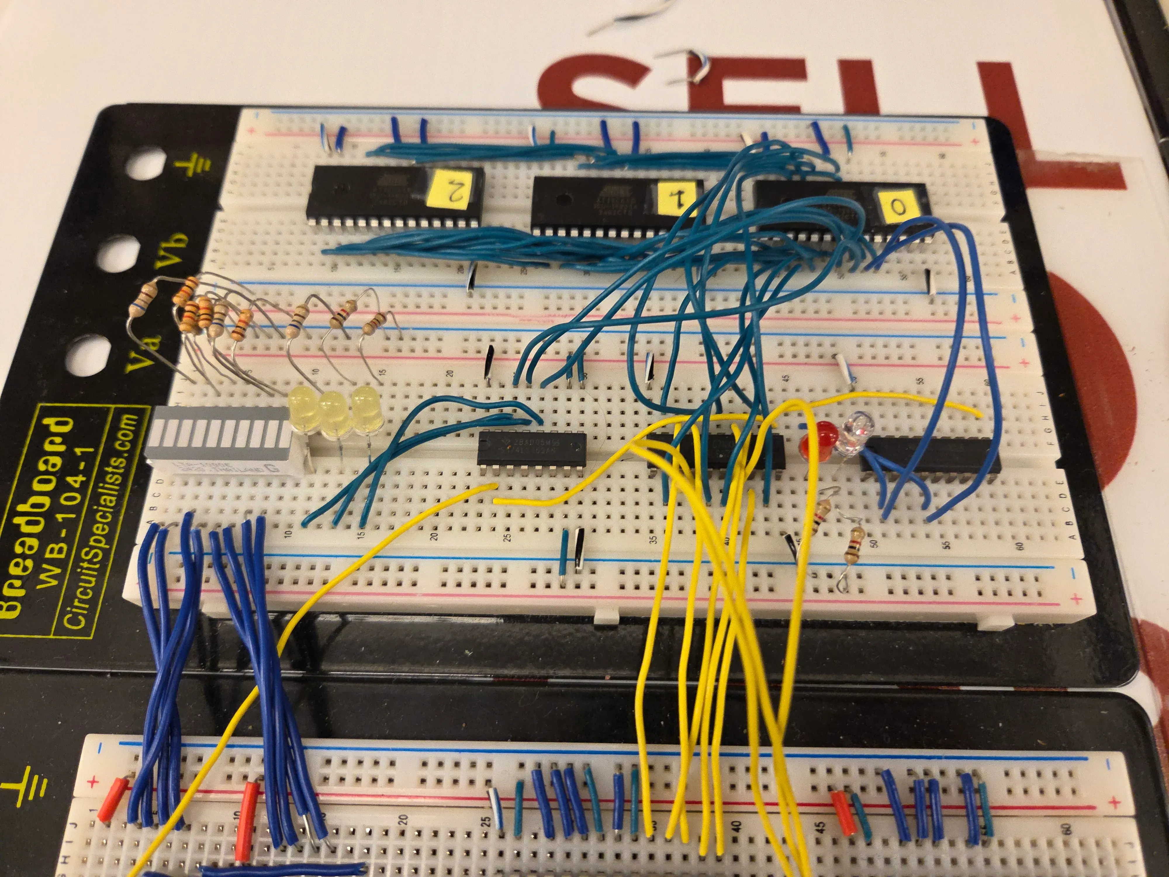
The rest of the wires
At this point, you can take away the rest of the wires, and you’ll be left with a pretty clean looking (nonfunctional) computer as well as a huge mess of wires.

Designing the computer and debugging
There is a lot more to talk about, but I’ll just talk about the process of designing, testing, and programming the computer.
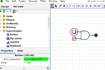
Before even assembling anything, we spent quite a while building it up in logisim. Only once our design was mostly finalized did we order the parts.
For debugging, it really helped to have a testing rig, both with 8 bit write/read, and 1 bit probes (which really helped later).
When we got everything on the bus, the writes and reads naturally moved onto the bus as well.
Software and programming
Programming the whole computer was about the same amount of work, if not more, compared to designing and building it. Since we used EEPROMs, all of the instruction decoding logic was pushed into software/our massive control signal spreadsheet.
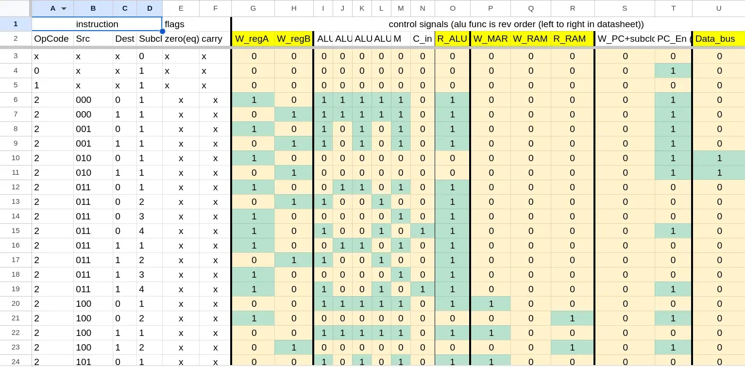
Additionally, Sagnik was in charge of flashing the EEPROMs with the control signal mappings and program data, as well as writing a compiler that could convert assembly into our instruction set.